Need for innovative connection solutions flourishes as control panels shrink in size
By Marc G Villeneuve, P. Eng., director sales & marketing, WECO
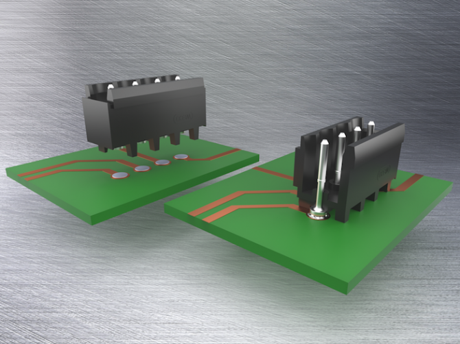
Electronics Interconnect IoT connector CTE IIoT Interconnect IoT pcb SMDSurface mount terminal blocks, connectors engineered for SMT assembly processes
Current technology has changed immensely in the last century and powering electrical controls have evolved exponentially. From the first industrial revolution with steam and water to power electricity and mass production, then to automation and CNC machining, and now to Industry 4.0 and IoT. The need for innovative connection solutions have flourished as control panels have shrunk in size resulting in increased power distribution over a smaller and densely populated printed circuit board (pcb).
As more sensors are used to monitor factory equipment, more signals need to be processed from a single power control board; the requirement for space-saving solutions becomes even more essential. In addition to high performance, the need to maximize pcb real estate is also of paramount importance. Surface mounted technology (SMT) is not only required to save space for signal connectors with low current, but equally important for power terminal blocks to supply power at a higher current. Soldering larger power terminal blocks and connectors using SMT reflow processes poses several challenges in the manufacturing environment.
Source: WECO
Ensuring a sound connection to the host pcb and a high ‘peel-off’ force for these large surface-mount-devices (SMD), key considerations needed to be addressed:
Process becomes intricate
First, one needs to consider the assembly of surface-mount-device (SMD) with varying size and weights. When soldering many components of different sizes to a surface mount board, the process becomes quite intricate. Large components such as magnetic components, and power terminal blocks, require a larger solder pad and a thicker layer of solder paste to ensure an adequate soldering. The requirements for a reliable solder joint require that each pin of an SMD make direct contact with the solder paste covering its respective solder pad.
Solder paste is deposited on the host pcb with a solder stencil and squeegee. The thickness of the solder stencil determines the thickness of the solder deposited. The thicker the solder paste, the more likely the SMD pin will make contact with the solder. During reflow, the surface tension properties of liquid solder cause the capillary action and the solder to wet between the pin and pad. Having components of various sizes requires selectively increasing the solder paste thickness where larger components are placed. This is often a challenge due to time constraints and can be difficult to achieve in a production environment. If the solder paste is too thick, there is a high probability of solder bridging for fine pitch components.
A second consideration is coplanarity, defined as the maximum distance between a surface-mount device (SMD) and its seating plane (the pcb). In essence, it is the physical contact point. When placed on a flat surface, a typical SMD will rest on its three lowest contact points. This defines the seating plane of the SMD. The maximum gap between the underside of any pin and the pcb is given a number for non-coplanarity. For large, complex components such as power terminal blocks, the ‘package coplanarity’ is often higher, meaning there is a greater variance between the seating plane of the terminal block and the pcb.
Connecting ‘pins’ in contact
Dealing with Coefficient of Thermal Expansion – (CTE) is the third key factor that will influence the reliability of the solder joint of a larger power terminal block or larger SMD device. Components of varying size, shape, material and weight all have different CTE and expand at different rates compared to smaller semiconductors. To achieve proper soldering, all components connecting ‘pins’ need to be in contact with the solder paste to allow the solder’s capillary action to form a proper solder joint. If the measured coplanarity of the pins is too great for the amount of solder deposited, some pins may not make contact with the solder paste. In this situation, the liquid solder simply forms a pool on the pcb pad. It does not wet to bridge the gap between the pin and pad, resulting in an electrical open circuit.
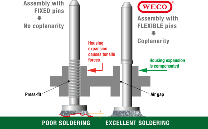
Pin strip assembly coplanarity. Source: WECO
WECO studied these issues and engineered SMarTconn, a portfolio of patented, field-tested, and robust connectors, terminal blocks, pins and anchoring with floating elements (or contacts) specifically designed for advanced SMT processes. The design considered solder paste requirements, coplanarity and varying coefficients of thermal expansion. Each contact is independent and able to ‘float’ within the terminal body. This principle of a floating elements allows an independent alignment of each contact to the pcb, ensuring coplanarity with the pcb surface, as well as ensuring a proper capillary action of the solder paste to wet and position each contact independently and therefore eliminating the CTE (coefficient of thermal expansion) mismatch during the reflow process.
Pull-Out-Force
Test plans were established to calculate and measure the long-term reliability of the soldered connections and the retention of the larger power terminal block to the pcb. The design considers the “Peel-Off Force”, “Pull-Out-Force” and “Torque Resistance”. For a Peel-Off test, the connector is pulled vertically (perpendicular to the pcb) and used to simulate the resistance on the ‘Z’ shape contacts and pcb solder. Recorded values with a 45º bending of the pins with a force of 18N (for a 4 pole – smaller 110-M-SMD series) resulted in no solder joint damage. Pull-Out-Force consist of pulling the complete housing vertically which simulates the resistance of the header to the pull-out-force generated by a mating plug. The header can be stressed to 180N for a 4 pole and to 200N for a 12 pole (smaller 110-M-SMD series) until the housing is separated for the pins with no damage to the pin solder joints. Torque resistance measures the robustness of the interface between the pcb solder pads and connector contacts. Connectors can be stressed over 50% higher than the torque applied to the screws securing the wires in the housings.
The principle of floating elements is also applied to the anchors. Similarly, to the individual contacts, floating anchors are aligned to the larger solder pads by capillary action and kept in place prior to the reflow solder process. Once soldered the terminal block is securely anchored to the pcb. The resulting Peel-Off-Force increases to 65N for the above mentioned smaller 110-M-SMD series connector.
All test values mentioned above are guidelines dependent on the quality of the solder joints, the pcb and process conditions.
———————————————
For an educational video on the principle of floating ‘elements’ or contacts please visit https://www.wecoconnectors.com/en/products/